external links:

![]()
 Embedded Artists
My First VHDL
18 September 2006: Not quite true
Ok, I should be honest: This is not my first vhdl design but it is the first test that I am creating from the bottom up ... You will find some weird constructions in the code but that's just because part of the exercise is to explore real problems that will appear in larger designs. |
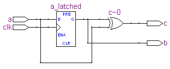
The design: it looks so simple ... This is it, the circuit shown is what will be created - it actually is the output of the RTL schematics viewer of Quartus.
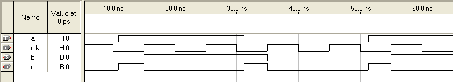
The output C will only be high from the time when input A changes to the next rising clock edge as can be seen from the timing diagram.
The clock signal CLK is driven with a 100 MHz signal. Output B follows A at every clock edge and C is only high from the time that A changes until the next rising clock edge. All this is created with a a few lines of VHDL code: LIBRARY IEEE; USE IEEE.std_logic_1164.ALL; entity all_mine is (1) port( clk : IN std_logic; a : IN std_logic; b : OUT std_logic; c : OUT std_logic ); end all_mine; architecture structure of all_mine is (2) signal a_latched : std_logic; begin b <= a_latched; (3) c <= a xor a_latched; latch_a : process (clk) (4) begin if rising_edge(clk) then a_latched <= a; end if; end process; end structure;
|
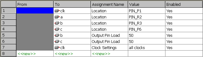
Compiling the code: the tedious job of specifying all constraints In order to compile the code you have to create a new project and add a file with the component to that project. There is a nice tutorial delivered with Quartus guiding you in doing so. During compilation some warnings will be shown to tell you that you have not specified a load capacitance for the output pins and that the CLK line is not assigned a clock setting. In order to get proper results from the timing analyses, these values should be given the appropriate values. If the output load is not specified the default load will be used - it's best to specify this value for each pin in order to prevent these warnings. Specifying the output pin load and clock settings is done in the Assignment Editor (from the Assignments menu):
The clock settings are specified using the Timing Analysis Settings (from the Assignments menu). Click on the 'Individual Clocks' button to specify clock frequency and duty cycle. I specified 66 MHz and 50% duty cycle. This resolved all warning during compilation.
|
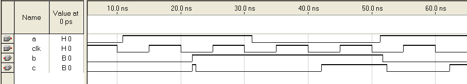
Simulating: not so simple after all ... In order to simulate the design the waveforms for the input signals have to be specified. This is done using the waveform editor as shown in the PDF tutorial from Altera. You only need to specify the A and CLK signals since the other signals are output. Now simulation can be started. In the Settings Editor (from the Assignments menu) there is a separate page with the Simulator Settings. Here you can select if you want a functional simulation or a full timing simulation. From the two simulation waveforms given below you will see that timing and pin loads have a real impact on the output.
Functional Simulation
Timing Simulation Compare these results with the different pages under the Timing Analyzer section in the compilation report. Look at the tco (clock to output times) and tpd (point to point delay) pages. Play around with this for some time and change the output load, clock frequency and try to add a second latch (in front of the current circuit). |
More to come Gaisler Research has a great IP library available under the GPL license, OpenCores.org also has some nice IP (not all IP on the site conforms to the same standards though) and this nice board from Gleichmann has some nice features that you will not quickly find in this price range. Enough material to fill a complete website ... |